

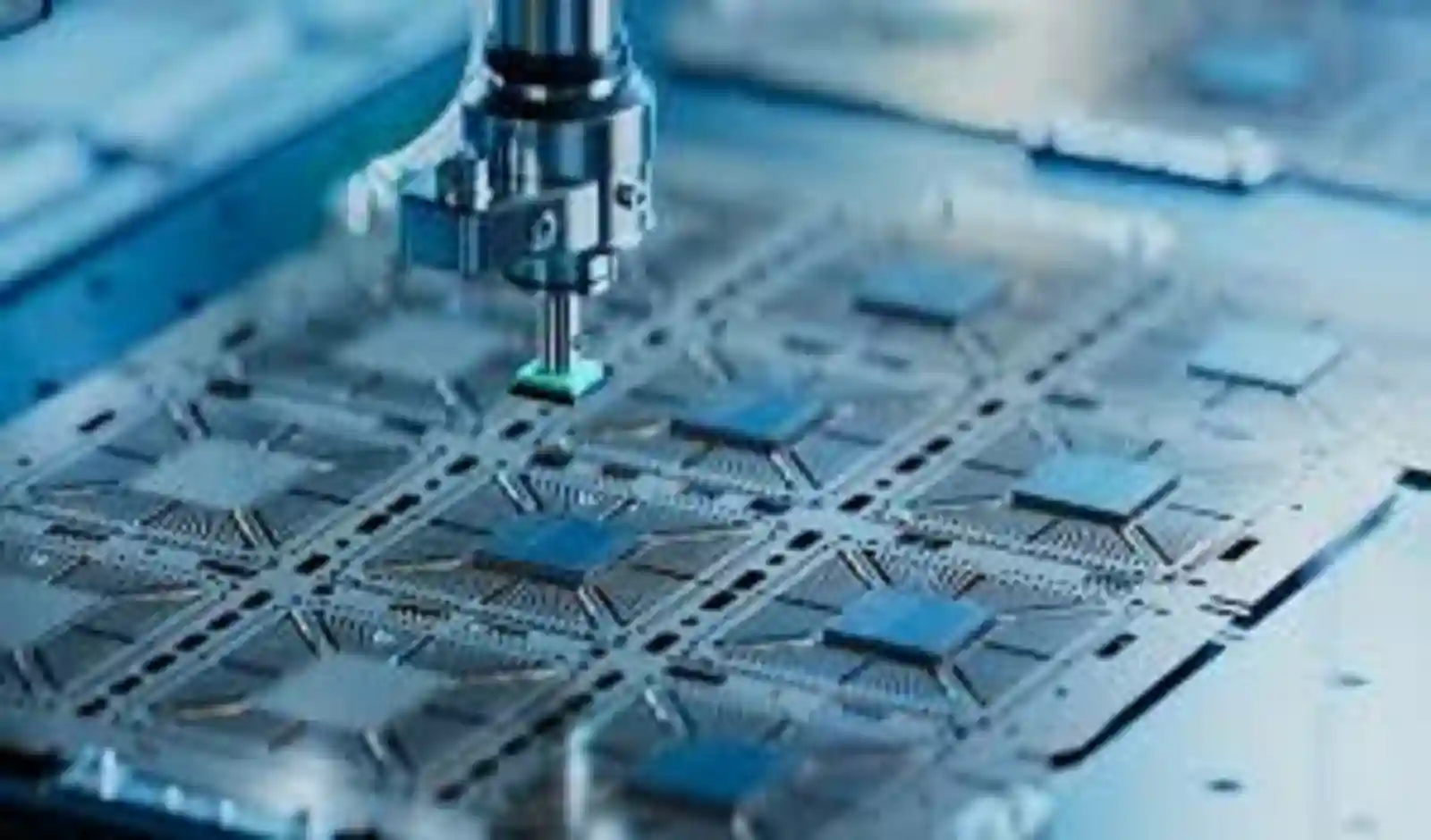
India is rapidly advancing its semiconductor ambitions, recognizing semiconductor chips as critical enablers of healthcare, transport, communications, defence, space, and emerging digital infrastructure. Semiconductor chip design is the main value driver, contributing up to 50 per cent of value addition and promoting intellectual property development, critical to strengthen India's position in the end to end value chain.
Globally, it contributes 30–35 per cent of global semiconductor sales through the fabless segment.
The Ministry of Electronics and Information Technology's (MeitY) Design Linked Incentive (DLI) Scheme under the Semicon India Programme aims to build a self-reliant, globally competitive chip design ecosystem, thereby establishing long-term technological leadership.
India has a strong presence in semiconductor design, approximately 20 per cent of the global integrated circuit (IC) design talent (estimated to range between 100,000 to 125,000) is here and India designs around 3,000-4,000 ICs each year.
India's DLI scheme catalyses the domestic semiconductor ecosystem by offering targeted financial incentives and advanced design infrastructure support across the full lifecycle of chip design.
"Fom IC and system-on-chips (SoC) development to deployment. It promotes indigenous content and intellectual property, reduces import dependence, and builds a high-end design base in India that is critical to strengthen India's position in the semiconductor value chain while enabling startups and MSMEs to innovate and scale," said Kathir Thandavarayan, Partner, Deloitte India.
"Design is also where the value lies over the long term. If you own the designs, you own the roadmaps. Fabrication can come second. Therefore, instead of playing catch-up globally, India can start where it already has a lead. The bright part about the DLI initiative is that it leverages what India already does well. Perhaps, we are not yet a major player in terms of having large fabs, but we definitely have an enormous pool of designers of chips working for MNCs. It provides an opportunity for them to do something other than export talent," said Devroop Dhar, cofounder and India CEO, Primus Partners.
In the electronics value chain, fabless semiconductor companies hold the highest strategic value because they design the chips that drive product intelligence, efficiency, and security. While fabs manufacture silicon and EMS firms assemble devices, more than half of a semiconductor's value comes from design and IP, not physical production. Fabless semiconductor design models generate high value addition with relatively modest capital expenditure, as design and IP contribute disproportionately to product economic value.
Without strong fabless capability, a nation remains dependent on imported core technologies even if electronics are manufactured locally. Building a robust fabless ecosystem therefore enables India to own the most critical layer of the value chain, retain intellectual property, reduce imports, attract manufacturing, and establish long-term technological leadership.
Under the DLI scheme, 24 chip-design projects have been sanctioned across areas such as video surveillance, drone detection, energy meters, microprocessors, satellite communications, and broadband and IoT SoCs. Additionally, 95 companies have received access to industry-grade EDA tools, significantly reducing design and infrastructure costs for Indian chip design startups, according to a statement by PIB.
By extending financial incentives, access to advanced design tools, and prototyping support to companies, startups, and academic institutions, the scheme enables innovators to progress seamlessly from ideas to actual silicon chips.
Amongst companies, large indigenous chip design firms can achieve better economies of scale that would give an edge with respect to the cost competitiveness.
"Design linked schemes should be extended to Indian domestic companies, in addition to startups and MSMEs, with provisions allowing companies to register multiple IPs at once, enabling faster scaling to meet India's semiconductor needs," Sandeep Kumar, CEO, LTSCT told Entrepreneur India in a previous interaction.
Keynes Semicon rolled out the first commercially manufactured complex chip from its Sanand OSAT facility in late 2025. "We would like to do complete backward integration and would get into design work with partners, as a beneficiary of the DLI scheme," said Raghu Panicker, CEO, Kaynes Semicon.
Coverage of large-scale Indian organizations under the DLI scheme can accelerate ecosystem growth given their enhanced R&D capacity, scale and market reach.
Devroop Dhar shares a different opinion. "The startups should remain the focus. Large firms can be very useful partners-helping with scale, customers, testing and going to market. If corporations are bought in as collaborators rather than beneficiaries, it strengthens the whole chain. Startups build the IP, larger firms help commercialise it. That is how we can move from good design talent to a real semiconductor ecosystem," Dhar explained.
Startups and MSMEs are eligible for financial incentives and design infrastructure support for semiconductor product design & deployment and other domestic companies are eligible for financial incentives for deploying semiconductor designs.
"Large-scale Indian organisation participation would enable faster commercialisation of advanced designs, enhance technology spillovers, and attract further investment into India's semiconductor value chain. The existing scheme covers domestic companies without any limit on the size," added Thandavarayan of Deloitte India.
 This article was originally
published by the
This article was originally
published by the