

This initiative is considered significant in strengthening the country’s semiconductor capabilities and advancing 'technology self-reliance.'
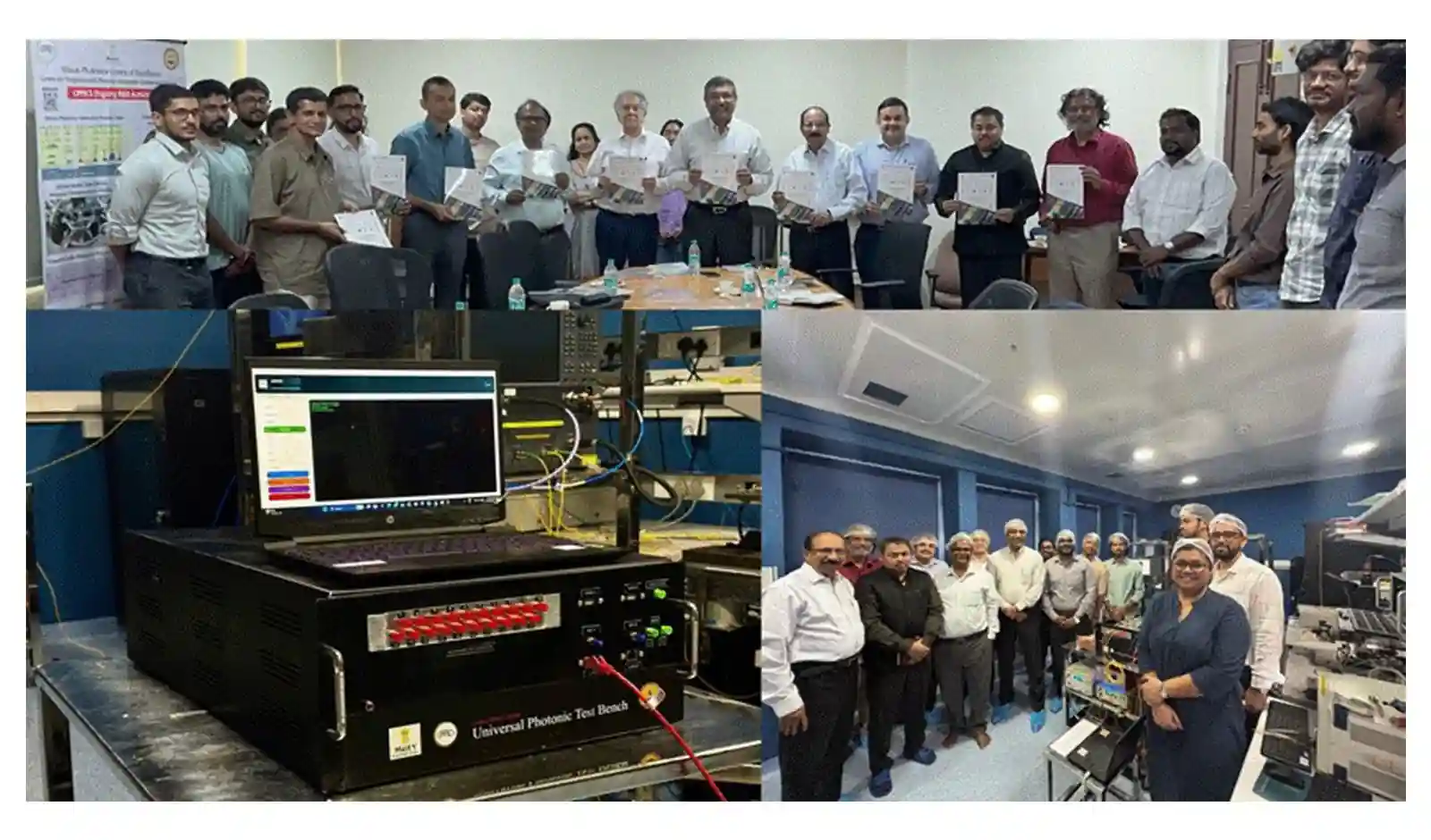
The technology was launched under the leadership of S. Krishnan, Secretary at the Ministry of Electronics and Information Technology (MeitY). During the event, two major innovations were introduced the Silicon Photonics Process Design Kit (PDK) and the Universal Programmable Photonic Integrated Circuit (PPIC) Test Engine. Both technologies have been developed at the MeitY-supported Centre of Excellence (CoE-CPPICS) at IIT Madras.
Silicon Photonics: A Technology of the Future
Silicon Photonics is a modern technology that integrates optical (light-based) and electronic components on a single chip. This technology is useful for high-speed data transfer, improved communication systems and advanced computing. The government believes that this development will make India globally competitive in this field.
The new solutions have been developed as a shared national platform to support research and development across educational institutions, industry, startups and defence organisations. This will provide students and researchers an opportunity to work on cutting-edge technologies and promote innovation.
PDK and PPIC to Boost Technological Advancement
The launched PDK includes more than 50 verified components, helping in the design of advanced photonic circuits. Meanwhile, the PPIC Test Engine is a modern automated platform used for testing and analysing photonic and optoelectronic modules.
Officials at the event stated that India’s Silicon Photonics capabilities are now approaching global standards. Amitesh Sinha, CEO of the India Semiconductor Mission, said that the technology has applications in both classical and quantum domains. Further research will be supported under the proposed ISM 2.0 initiative.
In the next phase of the project, multi-project wafer (MPW) fabrication will begin from the third quarter of the current financial year. This phase will include manufacturing, testing, packaging and module characterisation, helping build a complete technology ecosystem in the country.
New Opportunities for Education and Employment
This initiative will not only boost technological development but also create new opportunities for students to learn skills and find employment. Young professionals in engineering and research will get exposure to advanced technologies, strengthening their capabilities and preparing them for global competition.
Overall, the development of indigenous Silicon Photonics technology at IIT Madras marks a significant milestone in making India self-reliant in the semiconductor and high-tech industry. This initiative will positively impact education, research, innovation and employment, accelerating the country’s economic and technological growth.